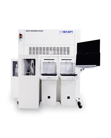
WAFER INSPECTION SYSTEM II
Model :GWIS-WM1000S
· A Wafer Transfer Robot(WTR) capable of stable handling for wafer thicknesses
below 200um, including Thinned & Warped Wafers
· A Rubber Chuck & Warpage Minimizer to prevent Micro Bump Damage
during Bumped Wafer Inspection
· Inspection of defects on the backside of wafers (cracks, chipping FM, BSC Void)
using a 16K Line Scan high-resolution camera
· Inspection of Wafer Marking Alignment using Two-Way Scope cameras
for simultaneous imaging of the Wafer Top and Bottom
· Load Port Module (8 & 12 Inch FOSB & Cassette)
· Wafer Transfer Robot (with Bernoulli Hand)
· Pre-Aligner (Wafer Notch Detection and Alignment)
· Wafer ID OCR (COGNEX IS1740 Series Reader)
· Minimizer and Rubber Chuck
(Specific Design And ESD Material Applied )
· Flipper (With Bernoulli Hand)
· Wafer Defect Inspection
(16K Line Scan Camera)
· Wafer Marking Alignment Inspection
(Top & Bottom Dual Camera)

X


